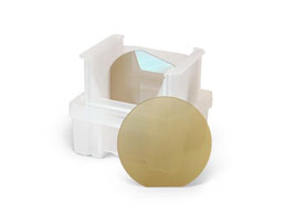
SILICON-ON-SAPPHIRE EPITAXIAL WAFERS
Silicon on Sapphire (SOS) Epitaxial Wafers
Epiel provides Silicon Epitaxy on ultrapure R-plane sapphire substrates. Silicon on sapphire epiwafers are mainly used as substrates for manufacturing electronic devices used in sensors, telecommunications, optoelectronics and other applications. Common applications include:
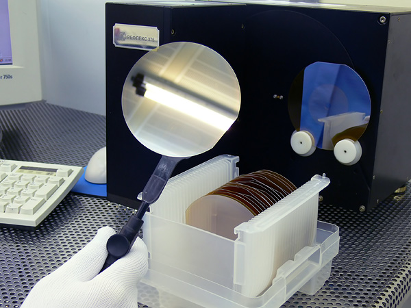
Lattice mismatch is the largest problem in silicon on sapphire growth causing structural defects in the transition from substrate to layer. Epiel's proprietary technology for epitaxial deposition of silicon on sapphire substrates enables the growth of low-defect ultra-thin monocrystalline doped layers suitable for integrated circuit manufacturing. Tipical layer thickness is less than 1 micron. Silicon on sapphire epiwafers are available in 76, 100 and 150 mm sizes. 200 mm is available at special request. |
Contact Sales Phone: +7 (499) 995 0049 E-mail: sales@epiel.ru |
| Parameters range for Silicon on Sapphire (SOS) Epi Wafers | |
|---|---|
| Wafer diameter | 76 mm, 100 mm, 150 mm |
| Orientation | (1012) ± 1º (R-plane) |
| Substrate dopant | - |
| Epi-layer thickness, µm | 0,3 – 2,0 |
| Epi-layer dopant | Phosphorous, Boron |
| Epi-layer resistivity, Ohm.cm |
|
| n-type | according to spec. |
| p-type | 1,0 – 0,01 |