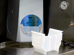
By the end of 2011 Epiel plans to finish the facility modernization project and introduce 200 mm Epi products for Power device and Integrated circuit applications
-
01.11.2010
As a leader on the Russian Silicon Epitaxy market Epiel carefully monitors the progress of the Russian microelectronics industry. In recent years much has been done by the leading semiconductor manufacturers to establish the basis for 180-90 nm microchip production on 200 mm wafers.
Epiel corporate development strategy focuses on maximizing customer satisfaction through improvement of the quality of Epi products and customer service and development of new Epi products designed to meet the customers’ new requirements. Penetrating the new 200 mm Epi wafer segment is a strategic goal for Epiel, which will enable the company to maintain the leading position on the Russian silicon epitaxy market.
To pursue this goal the company has been developing a comprehensive facility modernization project. The project aims to increase overall Epi wafer production capacity and introduce 200 mm Epi products for Power device and Integrated circuit applications to fulfill the needs of the leading Russian semiconductor manufacturers. In addition Epiel plans to expand its export operations by offering 200 mm Epi products to customers worldwide.
Preproject investigations have been completed, project implementation will take place in Q1-Q4 2011. In Q1 2012 Epiel plans to set the new facility in operation, gradually increasing capacity utilization.
To develop the technological basis for the project Epiel has conducted indoor research and development encompassing material research and process investigations for silicon Epi deposition on 200 mm wafers.
Although the technological equipment currently available at Epiel is capable of processing 200 mm wafers it does not allow for economically effective series production of 200 mm Epi wafers. The modernization project features installation of new high-class equipment units at every technological step including wafer preparation, epitaxial deposition and parameter control.
Facility design and equipment set were elaborated in close cooperation with industry experts to ensure that the new manufacturing line is well balanced and optimized for series production of 200 mm Epi wafers. Consulting support was provided by Silicon Quest International (USA), The Production and Engineering Management Group (USA).


