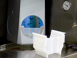
Epiel introduces 200 mm Silicon Epi wafers for Power Electronics
-
17.01.2013
While the global IC and microprocessor industry is shifting to large wafer sizes (300 and 450 mm) in the discrete power device sector 150 and 200 mm wafers are still the standard. With the recent introduction of 200 mm N-type silicon wafers the power device industry has started shifting from 150 mm wafers to 200 mm. Major drivers are cost efficiency and higher throughput.
Following the global trend Epiel introduces 200 mm Silicon Epi wafers for discrete power devices. In our 150-200 mm facility we utilize field proven high throughput Epi deposition equipment used by some of the world’s leading semiconductor manufacturers. Our equipment provides excellent layer quality and unique process characteristics for thick Epi applications.
The global Power Semiconductor device market is estimated at USD 13-15 bn (5% of the world semiconductor market) and demonstrates stable annual growth. The fastest growing segment is IGBT (over USD 1 bn) which are manufactured on thick layer silicon epi wafers. The growth is largely driven by a boom for energy efficient technologies – hybrid vehicles, industrial motor drives and solar energy system inverters, to name a few.
For details, please, see Silicon Epitaxy


