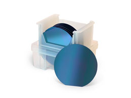
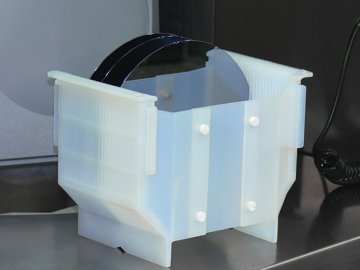
Silicon Epitaxial Wafers
Silicon Epitaxial Wafers
| Silicon Epitaxial Wafers are the core material used in manufacturing of a wide range of semiconductor devices with applications in consumer, industrial and space electronics.
Epiel provides a variety of production proven and industry standard Silicon Epitaxy process technologies for some of the most essential microelectronics applications: Diodes
Transistors
Integrated Circuits
To Integrated Circuit manufacturers Epiel offers Silicon Epitaxial Deposition Services on substrates with burried ion-implanted or diffused layers. Silicon substrates are either purchased from major global vendors or supplied by customer.
|
Contact Sales Phone: +7 (499) 995 0049 E-mail: sales@epiel.ru |

| Parameters range for Silicon Epi Wafers | |
|---|---|
| Wafer diameter | 76 mm, 100 mm, 150 mm, 200 mm |
| Orientation | (111), (100) |
| Substrate dopant | Antimony, Boron, Arsenic |
| Epi-layer thickness, µm | 3,0 – 150 |
| Epi-layer dopant | Phosphorous, Boron, Arsenic |
| Epi-layer resistivity, Ohm.cm |
|
| n-type | 0,01 – 500 |
| p-type | 0,01 – 100 |
| Single-layer structure types | n-n+, p-n+, p-p+, n-p+ |
| Double-layer structure types | n1-n2-n+, n1-n2-p+, n-p-n+, p-n-p |
| Buried Layer Epi | Up to 3 buried layers |